- 您现在的位置:买卖IC网 > Sheet目录317 > C8051F930-TB (Silicon Laboratories Inc)BOARD TARGET/PROTO W/C8051F930
�� �
�
�C8051F93x/92x�
�5.� Target� Board�
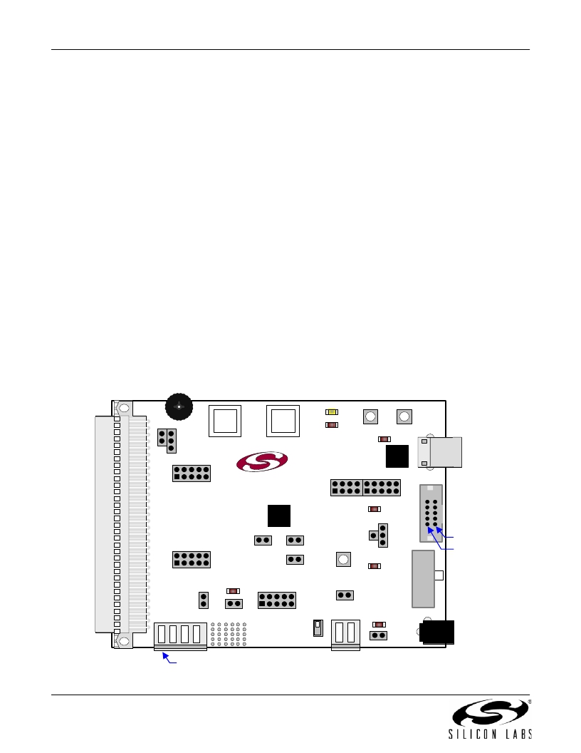
�The� C8051F930� Development� Kit� includes� a� target� board� with� a� C8051F930� device� pre-installed� for� evaluation� and�
�preliminary� software� development.� Numerous� input/output� (I/O)� connections� are� provided� to� facilitate� prototyping�
�using� the� target� board.� Refer� to� Figure� 8� for� the� locations� of� the� various� I/O� connectors.� Figure� 10� on� page� 12�
�shows� the� factory� default� shorting� block� positions.�
�P1�
�P2�
�P3�
�J1�
�J2,� J3,� J4�
�J5�
�J6�
�J7�
�J8�
�J9�
�J10,� J11�
�J12�
�J13�
�J14�
�J15�
�J16�
�J17�
�H1�
�H2�
�SW4�
�SW5�
�Expansion� connector� (96-pin)�
�Power� connector� (accepts� input� from� 7� to� 15� VDC� unregulated� power� adapter)�
�USB� connector� (connects� to� PC� for� serial� communication)�
�Enable/Disable� VBAT� Power� LED�
�Port� I/O� headers� (provide� access� to� Port� I/O� pins)�
�Enable/Disable� VDD/DC+� Power� LED�
�Provides� an� easily� accessible� ground� clip�
�Connects� pin� P0.7� (IREF0� Output)� to� resistor� R14� and� capacitor� C19�
�Connects� P0.2� and� P0.3� to� switches� and� P1.5� and� P1.6� to� LEDs�
�DEBUG� connector� for� Debug� Adapter� interface�
�Selects� the� power� supply� source� (Wall� Power,� AAA� Battery,� or� Coin� Cell)�
�Connects� Port� I/O� to� UART0� interface�
�Connects� external� VREF� capacitor� to� the� P0.0/VREF�
�Connects� the� PCB� ground� plane� to� P0.1/AGND�
�Connects� negative� potentiometer� (R14)� terminal� to� pin� P1.4� or� to� GND�
�Connects� the� potentiometer� (R14)� wiper� to� P0.6/CNVSTR�
�Creates� an� open� in� the� power� supply� path� to� allow� supply� current� measurement�
�Analog� I/O� terminal� block�
�Provides� terminal� block� access� to� the� input� and� output� nodes� of� J17�
�Switches� the� device� between� One-Cell� (0.9–1.8� V� supply)� or� Two-Cell� (1.8–3.6� V)� mode�
�Turns� power� to� the� MCU� on� or� off�
�P1.5� SW2�
�R15�
�J16�
�P1.4�
�J15�
�P1.6� P0.2� P0.3�
�SW3�
�USB� POWER� P3�
�GND�
�TOUCH� SENSE� SWITCH�
�P2.0�
�TOUCH� SENSE� SWITCH�
�P2.1�
�CP�
�2103�
�PORT2�
�J4�
�SILICON� LABS�
�www.silabs.com�
�J8�
�U3�
�J12�
�J9�
�U1�
�+1VD�
�P1�
�F930�
�COIN_CELL�
�J11�
�J13�
�PORT1�
�J3�
�J7�
�AAA_BAT�
�WALL_PWR�
�SW1�
�J14� +3VD�
�VBAT�
�Pin� 1�
�Pin� 2�
�RESET�
�J6�
�VDD/DC+�
�PORT0�
�IMEASURE�
�J5�
�`�
�J2�
�J17�
�OFF�
�H2�
�VBAT�
�SW4�
�H1�
�ON�
�SW5�
�J1�
�P2�
�Pin� 1�
�Figure� 8.� C8051F930� Target� Board�
�10�
�Rev.� 0.6�
�发布紧急采购,3分钟左右您将得到回复。
相关PDF资料
C8051T610DB24
DAUGHTER BOARD T610 24QFN SOCKET
C8051T630DB20
BOARD SOCKET DAUGHTER 20-QFN
CAN-100
BOARD EVAL RS232 100QFP
CANADAPT28
KIT ADAPTER CANDEMOBOARD 28PLCC
CAT24AA01WI-GT3
IC EEPROM SERIAL 1KB I2C 8SOIC
CAT24AA02WI-G
IC EEPROM SERIAL 2KB I2C 8SOIC
CAT24C01ZI-G
IC EEPROM SERIAL 1KB I2C 8MSOP
CAT24C03WI-G
IC EEPROM SERIAL 2KB I2C 8SOIC
相关代理商/技术参数
C8051F931
制造商:SILABS 制造商全称:SILABS 功能描述:25 MIPS, 8 kB Flash, Ultra Low Power, Capacitive Sensing MCU
C8051F931-F-GM
制造商:Silicon Laboratories Inc 功能描述:64KB,10ADC,24PIN MCU (LEAD FREE) - Rail/Tube 制造商:Silicon Laboratories Inc 功能描述:MCU 64KB FLASH 10BIT ADC 24QFN
C8051F931-F-GMR
制造商:Silicon Laboratories Inc 功能描述:64KB,10ADC,24PIN MCU - Tape and Reel 制造商:Silicon Laboratories Inc 功能描述:IC MCU 64KB FLASH 24QFN
C8051F931-G-GM
制造商:Silicon Laboratories Inc 功能描述:64KB/4KB RAM, 10B ADC, DC-DC, 0.9V, QFN24 - Rail/Tube 制造商:Silicon Laboratories Inc 功能描述:IC MCU 8BIT 64KB FLASH 24QFN
C8051F931-G-GMR
制造商:Silicon Laboratories Inc 功能描述:64KB/4KB RAM, 10B ADC, DC-DC, 0.9V, QFN24 - Tape and Reel 制造商:Silicon Laboratories Inc 功能描述:IC MCU 8BIT 64KB FLASH 24QFN
C8051F931-GM
功能描述:8位微控制器 -MCU 64KB 10ADC MCU LEAD FREE
RoHS:否 制造商:Silicon Labs 核心:8051 处理器系列:C8051F39x 数据总线宽度:8 bit 最大时钟频率:50 MHz 程序存储器大小:16 KB 数据 RAM 大小:1 KB 片上 ADC:Yes 工作电源电压:1.8 V to 3.6 V 工作温度范围:- 40 C to + 105 C 封装 / 箱体:QFN-20 安装风格:SMD/SMT
C8051F931-GMR
功能描述:8位微控制器 -MCU 64KB 10ADC MCU LEAD FREE
RoHS:否 制造商:Silicon Labs 核心:8051 处理器系列:C8051F39x 数据总线宽度:8 bit 最大时钟频率:50 MHz 程序存储器大小:16 KB 数据 RAM 大小:1 KB 片上 ADC:Yes 工作电源电压:1.8 V to 3.6 V 工作温度范围:- 40 C to + 105 C 封装 / 箱体:QFN-20 安装风格:SMD/SMT
C8051F93X
制造商:未知厂家 制造商全称:未知厂家 功能描述:Single/Dual Battery, 0.9–3.6 V, 64/32 kB, smaRTClock, 10-Bit ADC MCU